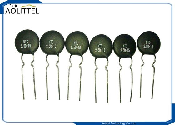
TUV Approved Low Profile 1608 Metric POLY-FUSE SMD Surface Mountable PTC Resettable Fuse EIA 0603 6V 500mA
Summary
(a) RoHS Compliant & Halogen Free
(b) Applications: All high-density boards
(c) Product Features: Small surface mountable, Solid state, Faster time to trip than standard SMD devices, Lower resistance than standard SMD devices
(d) Operation Current: 500mA
(e) Maximum Voltage: 6VDC
(f) Temperature Range : -40℃ to 85℃
Agency Recognition
TUV
UL
CSA
______________________________________________________________________________ Download________
Working Principle
FSMD Series PTC provides surface mount overcurrent protection for applications where space is at a premium and resettable protection is desired.
Electrical Characteristics (23℃)
| P/N |
(A) |
(A) |
(V) |
(A) |
Max. Trip |
(W) |
(Ω) |
| IH |
IT |
Vmax |
Imax |
(A) |
(Sec.) |
Pd typ |
Rmin |
R1max |
| FSMD010 |
0.10 |
0.30 |
15 |
40 |
0.50 |
1.00 |
0.50 |
0.90 |
6.00 |
| FSMD020 |
0.20 |
0.50 |
9 |
40 |
1.00 |
0.60 |
0.50 |
0.55 |
3.50 |
| FSMD035 |
0.35 |
0.75 |
6 |
40 |
8.00 |
0.10 |
0.50 |
0.20 |
1.40 |
| FSMD050 |
0.50 |
1.00 |
6 |
40 |
8.00 |
0.10 |
0.50 |
0.10 |
0.80 |
H=Hold current-maximum current at which the device will not trip at 23℃still air.
IT=Trip current-minimum current at which the device will always trip at 23℃ still air.
V MAX=Maximum voltage device can withstand without damage at it rated current.(I MAX)
I MAX= Maximum fault current device can withstand without damage at rated voltage (V MAX).
Pd=Typical power dissipated-type amount of power dissipated by the device when in the tripped state in 23℃ still air environment.
RMIN=Minimum device resistance at 23℃ prior to tripping.
R1MAX=Maximum device resistance at 23℃ measured 1 hour after tripping or reflow soldering of 260℃ for 20 seconds. Termination pad characteristics Termination pad materials: Pure Tin
Dimension (Unit:mm)
| P/N |
Marking |
A |
B |
C |
D |
| Min. |
Max. |
Min. |
Max. |
Min. |
Max. |
Min. |
| FSMD010 |
1 |
1.45 |
1.85 |
0.65 |
1.05 |
0.30 |
0.65 |
0.20 |
| FSMD020 |
2 |
1.45 |
1.85 |
0.65 |
1.05 |
0.30 |
0.65 |
0.20 |
| FSMD035 |
3 |
1.45 |
1.85 |
0.65 |
1.05 |
0.30 |
0.65 |
0.20 |
| FSMD050 |
5 |
1.45 |
1.85 |
0.65 |
1.05 |
0.65 |
1.00 |
0.20 |
Material Specification
Terminal pad material: Pure Tin
Soldering characteristics: Meets EIA specification RS 186-9E, ANSI/J-std-002 Category 3
Thermal Derating Curve
Typical time to trip at 25℃
The Time to Trip curves represent typical performance of a device in a simulated application environment. Actual performance in specific customer applications may differ from these values due to the influence of other variables.
Thermal Derating Chart – I hold (Amps)
| P/N |
Ambient Operating Temperature |
| -40℃ |
-20℃ |
0℃ |
25℃ |
40℃ |
50℃ |
60℃ |
70℃ |
85℃ |
| FSMD010 |
0.13 |
0.12 |
0.11 |
0.10 |
0.08 |
0.07 |
0.06 |
0.05 |
0.03 |
| FSMD020 |
0.27 |
0.25 |
0.23 |
0.20 |
0.17 |
0.14 |
0.12 |
0.10 |
0.07 |
| FSMD035 |
0.47 |
0.41 |
0.38 |
0.35 |
0.29 |
0.26 |
0.24 |
0.20 |
0.14 |
| FSMD050 |
0.67 |
0.59 |
0.54 |
0.50 |
0.41 |
0.37 |
0.34 |
0.29 |
0.20 |

 Your message must be between 20-3,000 characters!